Without going into complete details of how a semiconductor works, there
are certain things we must know about them in order to use them.
Semiconductors are chemical elements, that when compounded with other
elements, have certain electrical characteristics.
¿what?
There are several types of semiconductive chemicals, to include but not
limited to, Silicon, Germanium, Selenium, and Copper Oxide.
Semiconductors do not normally conduct electrical current. But when
they are combined with other chemicals, like Boron or Arsenic, can be
made to partially conduct. When we combine the second chemical to the
semiconductive chemical, we say that the semiconductor is "doped".
Doping can either be negative doping, or positive doping. The real
magic occurs, though, when we put the two types together.
 In
the diagram to the right, we see a device with both a positively and
negatively doped section joined. The point at which the two sections
join, we will call the N - P junction ( or simply the junction ). In
the diagram to the right, we see a device with both a positively and
negatively doped section joined. The point at which the two sections
join, we will call the N - P junction ( or simply the junction ).
Think of the junction as a hill, and the electrons flowing through it as
a ball. As long as the ball is rolling down hill, it is easy to push
along. But try pushing the ball uphill, and it is much harder to do.
The same goes with the flow of electricity through a junction of P and N
doped semiconductor material.

Consider, for a moment, what happens if we connect a negative DC voltage
to the N doped side, and a positive DC voltage to the P doped side.
According to the electron theory of current flow, electrons move from
negative to positive. The electrons leave from the negative side of the
battery, moving toward the positive. They come into contact with the
diode, which acts like a "hill" to the electrons. The electrons flow
"downhill", and current flows easily. But what happens if we reverse
the direction of current flow by reversing the battery?
 If the battery is reversed, the polarity applied to the diode also
changes. Electrons still try to flow from negative to positive,
however, going through the diode, is more like rolling a ball up-hill.
It takes much more effort to push the ball uphill. The hill is steepest
at the point of the P - N Junction, where it is nearly impossible to
push the ball up the hill.
If the battery is reversed, the polarity applied to the diode also
changes. Electrons still try to flow from negative to positive,
however, going through the diode, is more like rolling a ball up-hill.
It takes much more effort to push the ball uphill. The hill is steepest
at the point of the P - N Junction, where it is nearly impossible to
push the ball up the hill.
Because of this, a semiconductor diode acts much like a vacuum tube
diode, as it conducts in one direction, while having a high resistance
to current flow in the opposite direction.
It is possible, however, to make a diode conduct electricity in reverse.
If a high enough voltage is applied across the junction ( which is
also sometimes called the "depletion region" ), it will conduct in the
reverse direction. Just like if you kick the ball hard enough, it will
eventually go over the top of the hill. However, when this happens, the
diode is no longer acting quite like a normal diode.
Some diodes are actually designed to be operated in this manner. These
are called " ZENER DIODES ". When an exact given reverse bias voltage (
12 Volts for instance ) is reached, the junction of the diode begins to
" break down ", and act like a piece of wire. It does not conduct
electricity only in one direction, but in both directions at this point.

 The semiconductor diode ( usually just called a " diode " ), is one of
the most important building blocks of modern electronics.
The semiconductor diode ( usually just called a " diode " ), is one of
the most important building blocks of modern electronics.
To the right is a picture and the schematic symbol for the diode. Note
that there is always a line, or band that circles around one end of the
diode. This line indicates which end of the diode the cathode, or
positive end is on. Sometimes instead of a line, there is a dot or some
other kind of indicating marker, but the cathode is always indicated,
as the proper polarity of a diode is crucial in a circuit.
In addition to what you've already learned about semiconductor diodes,
most semiconductor devices have other properties that we have not
discussed. For instance, many semiconductor materials will radiate
light when electricity is passing through it.  This
is the principle behind how a Light Emitting Diode, or LED (schematic
to the right) works. The first case of this may be by H. J. Rounds, an
employee of Marconi Labs, who in 1907 made note of a light coming from a
Cat's Whisker connected to a crystal of silicon carbide. This
is the principle behind how a Light Emitting Diode, or LED (schematic
to the right) works. The first case of this may be by H. J. Rounds, an
employee of Marconi Labs, who in 1907 made note of a light coming from a
Cat's Whisker connected to a crystal of silicon carbide.
While knowledge of this wasn't kept a secret, and experimentation was
done on it for years, it wouldn't be until 1962 when General Electric
employee Nick Holonyak made a practical LED public, and from there it
took off. Light Emitting Diodes generate more light than heat, so unlike
a standard incandescent lamp, the LED used less electricity. This made
it ideal for battery operated devices that needed some kind of light
display. In addition, because it was so small, several of them could be
put in an array, making a display for characters (numbers and letters)
more readily available.
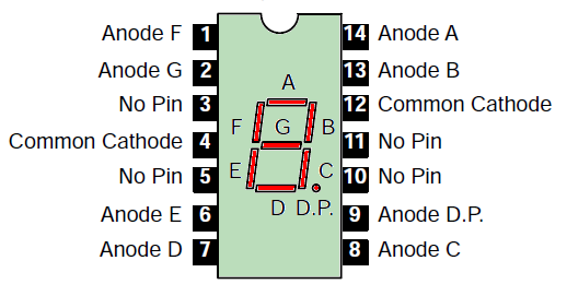
 This gives rise to the infamous "Seven Segment Display". The seven
segment display is used on all kinds of electronic equipment to display
basic letters and numbers.
This gives rise to the infamous "Seven Segment Display". The seven
segment display is used on all kinds of electronic equipment to display
basic letters and numbers.
It works by grounding one common leg of the display, while supplying
voltage (typically 5 volts) to other various legs. For instance, in the
display to the left, if we wanted to create the number 3, we would
ground pins 4 & 12, while supplying power to pins 2,7,8,13, and 14,
which would light up segments A, B, C, D, and G.
Another interesting feature of semiconductors, although not un-related,
is that it will conduct and/or generate electricity when light is
applied to it. this is the basis for the photoelectric cell (photocell -
you may relate to the Solar Cell). We will discuss this in more detail
in the section on transistors.
|