Featured Post

High CMRR Instrumentation Amplifier (Schematic and Layout) design for biomedical applications

Instrumentation amplifiers are intended to be used whenever acquisition of a useful signal is difficult. IA’s must have extremely high input impedances because source impedances may be high and/or unbalanced. bias and offset currents are low and relatively stable so that the source impedance need not be constant. Balanced differential inputs are provided so that the signal source may be referenced to any reasonable level independent of the IA output load reference. Common mode rejection, a measure of input balance, is very high so that noise pickup and ground drops, characteristic of remote sensor applications, are minimized.Care is taken to provide high, well characterized stability of critical parameters under varying conditions, such as changing temperatures and supply voltages. Finally, all components that are critical to the performance of the IA are internal to the device. The precision of an IA is provided at the expense of flexibility. By committing to the one specific task of

Simple Voltage Multiplier Circuit Diagram

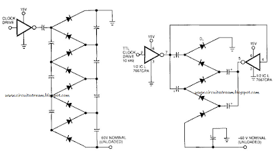
This is a Simple Voltage Multiplier Circuit Diagram. This Simple Voltage Multiplier Circuit Diagram we build to day. how to build lets start. Figure 99-l(a)`s circuit exhibits a high-output impedance as a result of the small effective capacitance of the series-connected capacitors, and it exhibits considerable voltage loss due to all of the diode drops. Further, this circuit requires 2 diodes and 2 capacitors to produce a dc output voltage approximately times the rail voltage. Figure 99-1 (b)`s circuit multiplies more effectively using fewer diodes and capacitors. 


Simple Voltage Multiplier Circuit Diagram


The parallel arrangement of the capacitors lets you use smaller capacitors than those required in Fig. 99-1(a). Alternatively, when using the same capacitor values of Fig. 99-1 (a), the output impedance will be lower. Whereas the clock source directly drives only one of the two strings of capacitors in Fig. 99-1(a), Fig. 99-l(b)`s clock drives both strings with opposite phases. 

This drive scheme doubles the voltage per stage of two diodes. A final diode is necessary to pick off the dc output voltage because both strings of capacitors now carry the - p ac input-voltage waveform. The ICL7667 dual-FET driver accepts a TTL drive swing and provides a low-impedance push-pull drive to the diode string. This low impedance is particularly helpful when using a long string to raise output voltage to more than 100 V, starting from a low rail voltage.  

Comments